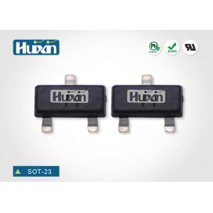
SOT-23 Plastic-Encapsulate MOSFETS
BSS138 N-Channel 50-V(D-S) MOSFET
FEATURES
1.High density cell design for extremely low RDS(on)
2.Rugged and Relaible
1.Direct Logic-Level Interface: TTL/CMOS
2.Drivers: Relays, Solenoids, Lamps, Hammers,Display, Memories, Transistors, etc.
3.Battery Operated Systems
4.Solid-State Relays
Maximum ratings (Ta=25℃ unless otherwise noted)
| Parameter | Symbol | Value | Unit |
| Drain-Source Voltage | VDS | 50 | V |
| Continuous Gate-Source Voltage | VGSS | ±20 |
| Continuous Drain Current | ID | 0.22 | A |
| Power Dissipation | PD | 0.35 | W |
| Thermal Resistance from Junction to Ambient | RθJA | 357 | ℃/W |
| Operating Temperature | Tj | 150 | ℃ |
| Storage Temperature | Tstg | -55 ~+150 |
ELECTRICAL CHARACTERISTICS (Ta=25 ℃ unless otherwise specified )
| Parameter | Symbol | Test Condition | Min | Typ | Max | Units |
| Off characteristics |
| Drain-source breakdown voltage | V(BR)DSS | VGS = 0V, ID =250µA | 50 | | | V |
| Gate-body leakage | IGSS | VDS =0V, VGS =±20V | | | ±100 | nA |
| Zero gate voltage drain current | IDSS | VDS =50V, VGS =0V | | | 0.5 | µA |
| VDS =30V, VGS =0V | | | 100 | nA |
| On characteristics |
| Gate-threshold voltage (note 1) | VGS(th) | VDS =VGS, ID =1mA | 0.80 | | 1.50 | V |
| Static drain-source on-resistance (note 1) | RDS(on) | VGS =10V, ID =0.22A | | | 3.50 | Ω |
| VGS =4.5V, ID =0.22A | | | 6 |
| Forward transconductance (note 1) | gFS | VDS =10V, ID =0.22A | 0.12 | | | S |
| Dynamic characteristics (note 2) |
| Input capacitance | Ciss | VDS =25V,VGS =0V, f=1MHz | | 27 | | pF |
| Output capacitance | Coss | | 13 | |
| Reverse transfer capacitance | Crss | | 6 | |
| Switching characteristics |
| Turn-on delay time (note 1,2) | td(on) | VDD=30V, VDS=10V, ID =0.29A,RGEN=6Ω | | | 5 | ns |
| Rise time (note 1,2) | tr | | | 18 |
| Turn-off delay time (note 1,2) | td(off) | | | 36 |
| Fall time (note 1,2) | tf | | | 14 |
| Drain-source body diode characteristics |
| Body diode forward voltage (note 1) | VSD | IS=0.44A, VGS = 0V | | | 1.4 | V |
Notes:
1. Pulse Test ; Pulse Width ≤300µs, Duty Cycle ≤2%.
2. These parameters have no way to verify.
